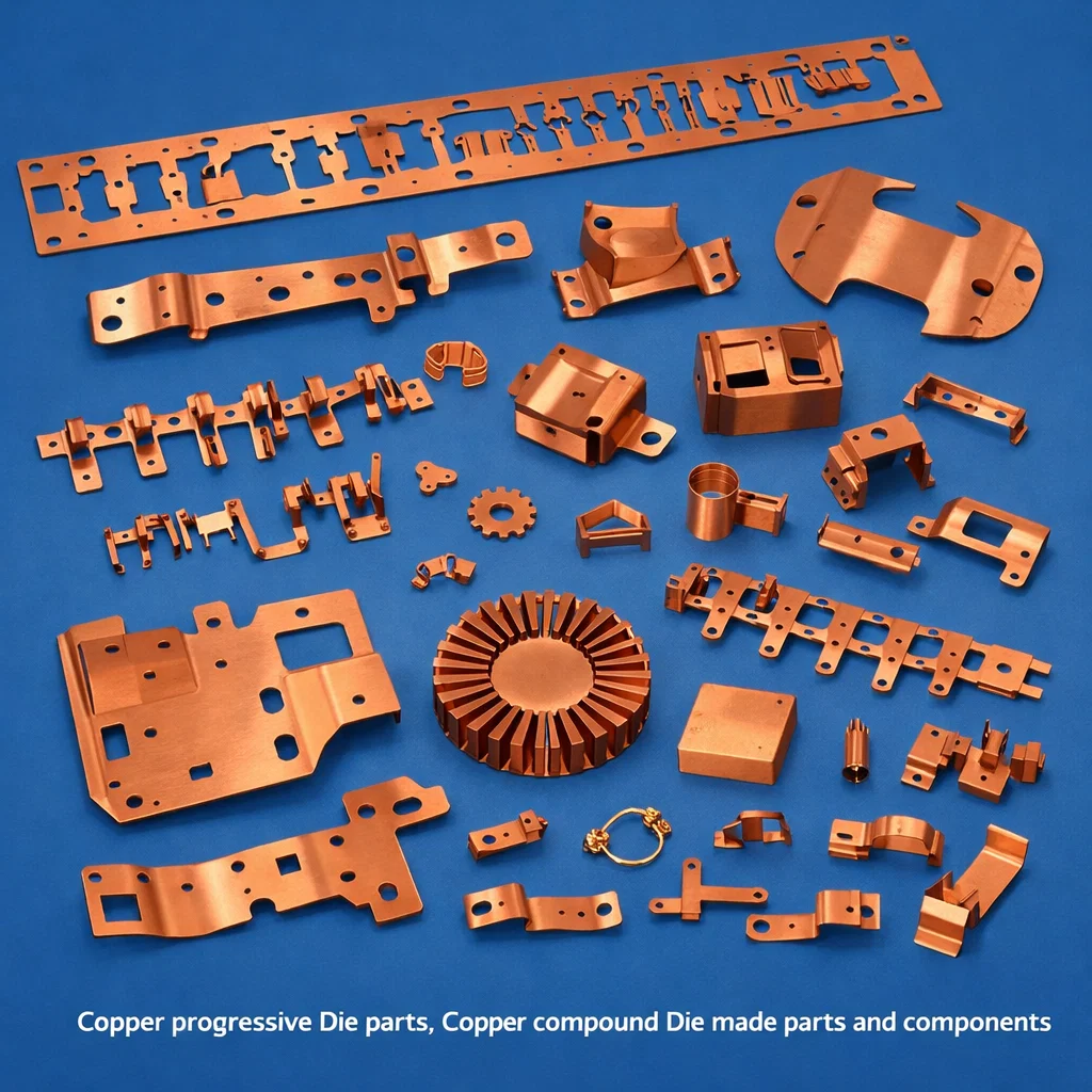
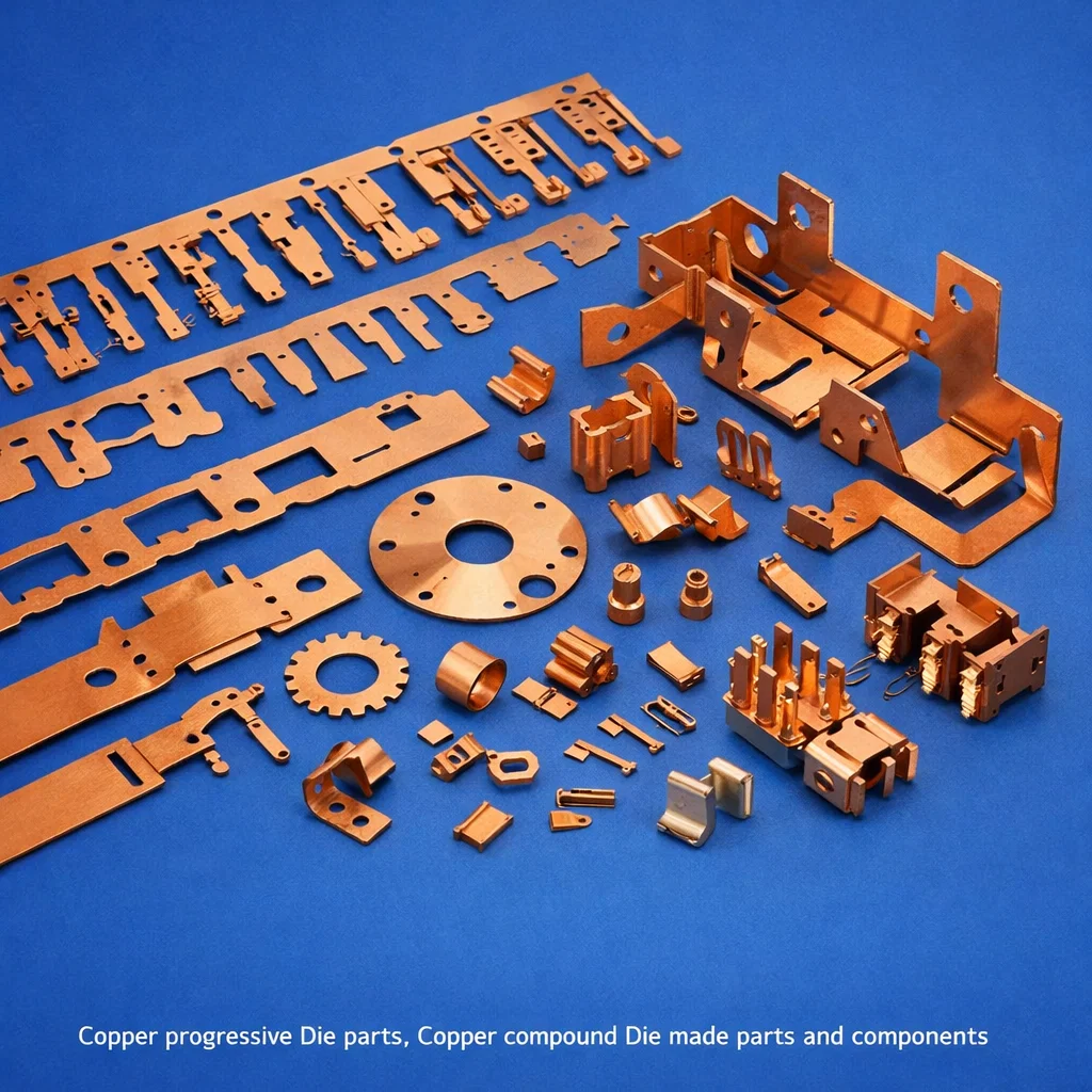
Copper Progressive Die & Compound Die Stamped Parts – Precision Copper Stampings Manufacturer

We are a specialist manufacturer and global exporter of Copper Progressive Die and Compound Die Stamped Parts, serving demanding industries including electrical, electronics, automotive, power distribution, renewable energy, telecommunications, and defence. With more than 30 years of hands-on copper stamping expertise, our factory produces ultra-precise copper pressed components that deliver outstanding electrical conductivity, thermal performance, and mechanical reliability.
Copper’s exceptional electrical conductivity (second only to silver) makes it the material of choice for busbars, terminal contacts, current-carrying clips, earthing components, and power connectors. Our progressive and compound die stamping processes handle copper strip from 0.1 mm to 6 mm thickness, producing complex multi-feature components in a single continuous operation — achieving tolerances as tight as ±0.01 mm and surface finishes down to Ra 0.8 µm.

Caption: Copper Progressive Die & Compound Die Stamped Parts – Precision Copper Stampings, India Manufacturer & Exporter
Why Copper for Stamped and Pressed Components?
Copper offers a unique combination of properties that make it irreplaceable in electrical and electronic applications. With an electrical conductivity of 58 MS/m (IACS 100%), thermal conductivity of 385 W/m·K, excellent corrosion resistance, and superb ductility for deep forming operations, copper stampings are the preferred choice for power connectors, busbar components, grounding clips, transformer contacts, motor winding supports, relay components, and battery terminals.
Copper Material Grades with International Equivalents
| Material | Indian IS | ASTM / UNS (USA) | EN / DIN (Europe) | BS (UK) | JIS (Japan) |
|---|---|---|---|---|---|
| Electrolytic Tough Pitch (ETP) Copper | IS 1897 Cu-ETP | C11000 | Cu-ETP / EN CW004A | C101 | C1100 |
| Oxygen-Free High Conductivity (OFHC) Copper | IS 1897 Cu-OF | C10100 / C10200 | Cu-OF / EN CW008A | C103 | C1020 |
| Phosphorus Deoxidized Copper (DHP) | IS 1897 Cu-DHP | C12200 | Cu-DHP / EN CW024A | C106 | C1220 |
| Silver-Bearing Copper | – | C11400 | CuAg0.1 / EN CW013A | C102 | C1401 |
| Beryllium Copper | – | C17200 | CuBe2 / EN CW101C | CB101 | C1720 |
| Tellurium Copper | – | C14500 | CuTeP / EN CW118C | C109 | C1450 |
Typical Size and Dimensional Capability – Copper Stampings
| Parameter | Compound Die (Copper) | Progressive Die (Copper) |
|---|---|---|
| Strip/Sheet Thickness | 0.2 mm – 6 mm | 0.1 mm – 4 mm |
| Maximum Part Envelope | 350 mm × 250 mm | 200 mm × 150 mm |
| Minimum Hole Diameter | 1.0× material thickness | 1.0× material thickness |
| Dimensional Tolerance | ±0.01 – ±0.05 mm | ±0.01 – ±0.05 mm |
| Flatness (after levelling) | ≤ 0.03 mm / 100 mm | ≤ 0.03 mm / 100 mm |
| Surface Finish | Ra 0.8 – 3.2 µm | Ra 0.8 – 3.2 µm |
| Annual Capacity | Up to 10 million pcs | Up to 60 million pcs |
Our Technical Expertise in Copper Die Stamping
Copper is a challenging material to stamp due to its high ductility and tendency to gall on die surfaces. Our engineers use specialized die coatings (TiN, TiAlN), polished die steels, and carefully designed clearances (typically 5–8% per side for copper) to achieve burr-free, clean-cut edges. Our CAD/CAM die design, in-house tool room, and automated strip feed systems guarantee consistently high-quality copper stampings even for thin-gauge and miniature components used in the electronics industry.
We have manufactured copper stampings for MV/LV switchgear busbars, solar panel junction box connectors, EV battery terminals, transformer tap changers, relay contact blades, motor terminal boards, and many other safety-critical applications where material integrity and dimensional consistency are non-negotiable.
Industries & Applications for Copper Stampings
Copper progressive and compound die stamped parts serve: Electrical switchgear, power distribution panels, transformers, motors & generators, solar energy systems, EV & hybrid vehicles, railway electrification, telecommunications infrastructure, industrial automation, and precision electronics manufacturing.
Performance Metrics – Copper Stamping Operations
| Metric | Our Standard |
|---|---|
| Electrical Conductivity (ETP Copper parts) | ≥ 99.9% IACS |
| Burr Height (cut edges) | ≤ 0.05 mm |
| Outgoing Defect Rate | < 30 PPM |
| Tooling Lead Time | 3–6 weeks |
| Sample Lead Time | 7–14 working days |
| Production Lead Time | 3–5 weeks post-approval |
| On-Time Delivery | 98.7% |
Why Choose Our Copper Stampings Over Competitors?
- Unmatched Copper Expertise: Dedicated copper press lines with specialized die coatings and lubrication systems — preventing galling, extending tool life, and delivering cleaner edges.
- 30+ Years of Export Experience: We understand the technical standards, documentation requirements, and logistics challenges of supplying to US, European, and Australian markets.
- Superior Communication: Dedicated account managers, engineering support in English and technical drawings support in metric and imperial units.
- Flexible Volumes: We cater to prototype (500 pcs) through high-volume production (millions per month).
- Full Traceability: Each batch comes with full mill certificates (chemical analysis, mechanical properties, conductivity), production records, and dimensional inspection reports.
- Secondary Operations Under One Roof: Plating (tin, silver, nickel), bending, assembly, and custom packaging — saving time and supply chain complexity for our customers.
- Competitive Lead Times: Faster than European and North American stamping shops due to India’s manufacturing efficiency and our decades of process optimization.
What Separates Us from Other Copper Stamping Manufacturers
Our focus on copper as a core material — not an afterthought — means our dies are designed specifically for copper’s unique springback, work hardening, and friction characteristics. We have invested in dedicated copper press lines with consistent-gap feeder systems, servo-controlled press speeds, and real-time tonnage monitoring. This level of specialization results in parts that consistently exceed customer expectations in both quality and value. Our zero-tolerance policy on customer complaints and our direct owner-managed engagement model mean every issue — if any — is resolved within 24 hours.
Our Flexibility to Customize Copper Stamped Parts
We manufacture copper stampings from customer drawings, samples, or sketches. We support all copper alloy grades, thicknesses from 0.1 mm, custom part marking (laser or ink), selective plating zones, multi-material assemblies (copper + brass + stainless), and special packaging such as reel-on-tape (for automated SMD pick-and-place), bulk bag, tray, or magazine feed. Engineering changes are accommodated rapidly — typically within 1–2 weeks for die modification.
Export-Worthy Packaging for Copper Parts
Copper parts are susceptible to surface oxidation and tarnishing. We use anti-tarnish VCI (Volatile Corrosion Inhibitor) poly bags, oxygen-free sealed packaging, and desiccant sachets for long sea-freight shipments. Parts are individually separated using inter-leaved tissue or plastic dividers to prevent contact corrosion. Export cartons are moisture-sealed, palletized, and labeled with full traceability data per customer requirements.
Customer Testimonials
“We’ve been importing copper busbar stampings from this company for five years now. The dimensional consistency batch after batch is remarkable, and the material certificates they provide are thorough and accurate. Our goods-in inspection rarely flags anything. Truly a world-class copper stamping supplier.”
— Michael Hargreaves, Quality Director, Australia
“As a manufacturer of MV switchgear, material quality and delivery reliability are everything. This supplier has delivered both consistently. Their progressive die copper contacts have been running in our assembly line for three years without a single non-conformance. Communication is professional, responsive, and genuinely helpful.”
— Hans-Peter Müller, Technical Procurement Lead, Germany
Top Q&A – Copper Progressive Die & Compound Die Stamped Parts
Q1: Which copper grade is best for electrical contact stampings?
A: C11000 (ETP Copper) is the standard choice for most electrical contacts due to its 99.9% IACS conductivity and good formability. For spring contacts requiring higher strength, C17200 Beryllium Copper is used. For high-temperature applications, silver-bearing copper C11400 is preferred.
Q2: Can you stamp OFHC copper for vacuum and semiconductor applications?
A: Yes. We stamp C10100 and C10200 OFHC copper for vacuum system components, electron beam equipment, and semiconductor processing parts. Full material traceability and conductivity certificates provided.
Q3: What is the smallest copper part you can produce?
A: We can produce miniature copper stampings from 0.1 mm strip as small as 2 mm × 2 mm, used as SMD spring contacts and micro-connector pins.
Q4: How do you prevent copper oxidation on stamped parts?
A: We use VCI packaging, and for parts requiring permanent oxidation prevention, we offer electroless tin plating, silver plating, or passivation treatments.
Q5: Can you produce copper busbars with multiple punched holes?
A: Yes. We produce copper busbars of any length, width, and thickness with punched holes, slots, notches, and formed features. Compound and progressive dies both used depending on design.
Q6: Do you offer silver-plated copper stampings?
A: Yes. Silver plating is available in thicknesses from 2µm to 25µm, applied selectively or fully, to improve contact resistance and solderability.
Q7: What is the maximum thickness of copper you can stamp?
A: Our presses can stamp copper up to 6 mm thickness in single-stroke compound operations. For progressive die work, up to 4 mm is standard.
Q8: Can you produce copper stampings with tight bend radii?
A: Yes. ETP and DHP copper can be formed to very tight bend radii (0.5× material thickness) due to their high ductility. Beryllium copper requires larger radii to avoid cracking.
Q9: What is your quality control process for copper stampings?
A: We perform 100% visual inspection, sampling CMM inspection per AQL, burr height measurement, conductivity testing (for ETP parts), and hardness testing (for BeCu parts).
Q10: Do you offer tin-plated copper stampings for PCB applications?
A: Yes. Bright tin plating, matte tin plating, and lead-free HASL-equivalent plating are available on copper stampings for PCB connector and terminal applications.
Q11: What industries commonly use copper progressive die stampings?
A: Electrical switchgear, transformer manufacturing, EV battery systems, solar energy, railways, industrial motors, PCB connectors, and telecommunications hardware.
Q12: Can you produce copper stampings with embossed logos or part numbers?
A: Yes. We can emboss, coin, or laser-mark part numbers, lot codes, and customer logos directly on copper stampings.
Q13: Do you offer sub-assembly services combining copper stampings with other materials?
A: Yes. We can assemble copper stampings with brass inserts, stainless steel springs, plastic housings, and other components as per customer requirements.
Q14: Can you reverse-engineer a copper stamped part from a sample?
A: Yes. We accept physical samples for reverse engineering. We perform 3D scanning or precision CMM measurement to create manufacturing drawings and tooling.
Q15: Are your copper stampings suitable for cryogenic applications?
A: Yes. OFHC copper (C10100/C10200) retains full ductility and conductivity at cryogenic temperatures and is widely used in superconducting and cryogenic equipment.
Glossary of Related Parts & Technical Terms
ETP Copper: Electrolytic Tough Pitch copper – the most common electrical-grade copper with 99.9% minimum purity and 100% IACS conductivity.
OFHC: Oxygen-Free High Conductivity copper – used in vacuum, cryogenic, and high-frequency applications requiring ultra-low impurity levels.
Springback: Elastic recovery of metal after stamping; more pronounced in beryllium copper and harder temper materials.
IACS: International Annealed Copper Standard – the benchmark for measuring electrical conductivity of metals relative to copper.
VCI Packaging: Volatile Corrosion Inhibitor packaging that releases corrosion-inhibiting vapor to protect metal surfaces during storage and transit.
Related Parts: copper busbar stampings, copper terminal blocks, copper connector plates, copper flat contacts, copper spring contacts, copper grounding clips, copper earth straps, copper lug stampings, copper heat sink blanks, copper EMI shielding parts, copper relay contacts, copper transformer tap changers, copper circuit breaker components, copper motor terminal plates, copper battery terminals, copper electrode blanks, copper SMD spring contacts, copper lead frames
Request a Quote – Copper Die Stamping Specialists
Need a reliable manufacturer for copper progressive die and compound die stamped parts? We are ready to review your drawings and deliver a fast, competitive proposal. Contact us now — your dedicated copper stamping specialist is available within 24 hours.
Product categories
Related Products
-

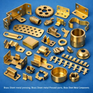
Brass Sheet Metal Pressed Parts and Pressed Components
Read more -
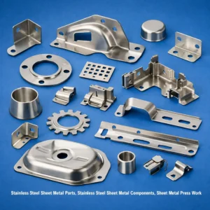
Stainless Steel Sheet Metal Parts
Read more -
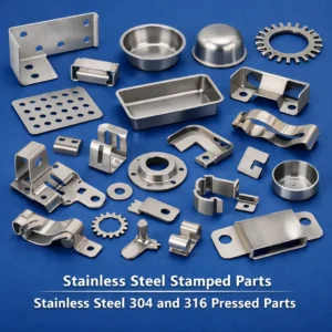
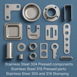
Stainless Steel Stamped Parts, Stainless Steel 304 and 316 Pressed Parts
Read more -
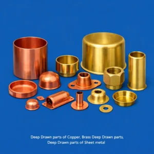
Copper Deep Drawn Parts, Brass Deep Drawn Parts
Read more -
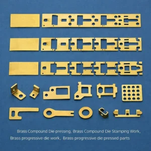
Compound and Progressive Die Stamping of Brass
Read more -
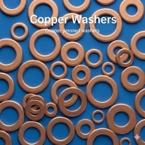
Copper Washers, Copper Sealing washers,
Read more -
Stainless Steel Pressed Parts & Stainless Steel Sheet Metal Components
Read more -
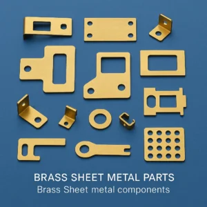
Brass Sheet Metal Parts, Brass Sheet metal Components
Read more -
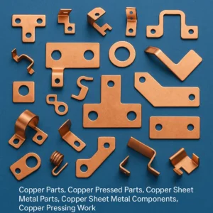
Copper Pressed Parts, Copper Sheet Metal Components
Read more -
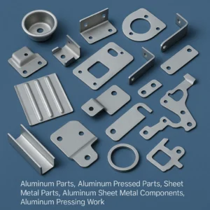
Aluminum Pressed Parts | Aluminum Sheet Metal Components
Read more -
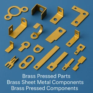
Brass Pressed Parts & Brass Pressed Components
Read more