Brass & Copper Parts is a leading manufacturer and exporter of precision copper transformer studs and copper studs for transformer bushings. We supply high-conductivity copper stud components to electrical equipment manufacturers, transformer OEMs, utilities, and electrical contractors across the USA and globally. Our transformer studs are engineered to deliver maximum electrical conductivity, exceptional mechanical strength, and long-term reliability in demanding power distribution and transmission environments.
What Are Copper Transformer Studs?
Copper transformer studs are precision-machined cylindrical copper components that serve as the primary current-carrying interface between a transformer’s internal winding and external electrical connections. They are typically inserted into or threaded into transformer bushings — the insulated terminals that penetrate the transformer tank wall or cover — and allow high-current connections to bus bars, cable lugs, and external circuit components.
The stud must provide minimum contact resistance, withstand mechanical clamping forces without deformation, resist thermal cycling, and maintain electrical integrity over decades of service. Only high-conductivity copper alloys, precisely machined and properly finished, meet these requirements.
Our Range of Copper Transformer Studs & Bushing Hardware
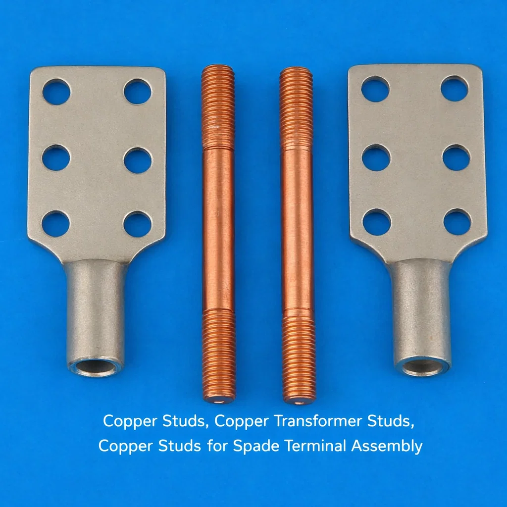
We manufacture a comprehensive range of copper stud components for transformer and high-voltage equipment applications:
Copper Bushing Studs (Standard & Custom)
Precision-turned copper studs for oil-filled, dry-type, and cast resin transformer bushings. Available in round, hexagonal, and custom profiles with threaded ends (UNC, UNF, Metric), smooth shank sections, and special shoulder geometries as required by the bushing design.
Double-Ended Copper Studs
Copper studs threaded at both ends with a smooth or hexagonal center section — used for connecting bushings to internal winding leads on one end and external bus bars or cable lugs on the other. Custom lengths and thread combinations available.
Copper Bushing Terminals & End Caps
Precision-machined copper bushing terminal caps, top caps, and end caps with machined flats, threaded holes, and cable bolt patterns for power transformer, instrument transformer, and switchgear bushing assemblies.
Copper Draw Leads & Draw Rods
High-conductivity copper draw lead assemblies and draw rods for oil-filled transformers — used to thread the winding lead through the bushing body. Available with eye bolts, threaded connectors, or swaged cable terminations.
Copper Clamp Bolts & Current-Carrying Hardware
Copper clamping bolts, nuts, washers, and hardware sets for transformer bushing assemblies and bus bar connections where current-carrying capacity must be maintained through all fastener elements in the current path.
Copper Bushing Current Transformers (CT) Stud Kits
Complete copper stud and hardware kits for bushing-type current transformer (BCT) installations on power transformers and switchgear, including studs, nuts, flat washers, and lock washers in ETP or tellurium copper.
Copper Tap Changer Studs & OLTC Components
Precision copper studs and contact components for on-load tap changer (OLTC) and de-energized tap changer (DETC) mechanisms in power transformers. Tight tolerances and specific alloy requirements for high-cycle contact performance.
Material Grades for Copper Transformer Studs — International Equivalents
All copper transformer studs from Brass & Copper Parts are manufactured from high-purity copper alloys selected for maximum electrical conductivity and machinability. The table below details the key grades and their international equivalents:
| Grade / Alloy | UNS (USA) | ASTM | BS (UK) | DIN / EN (Europe) | JIS (Japan) | Conductivity (% IACS) | Application |
|---|---|---|---|---|---|---|---|
| Electrolytic Tough Pitch (ETP) Copper | C11000 | B187, B133 | C101 | 2.0065 / E-Cu58 | C1100 | >100% | Standard bushing studs, bus bars |
| Oxygen-Free Electronic (OFE) Copper | C10100 | B170 | C103 | 2.0070 / OF-Cu | C1011 | >101% | High-vacuum, specialty HV bushings |
| Oxygen-Free Copper (OFC) | C10200 | B170 | C103 | 2.0076 / OF-Cu | C1020 | ~100% | Power transformer studs |
| Phosphorus Deoxidized Copper | C12200 | B152 | C106 | 2.0090 / SW-Cu | C1220 | ~85% | Solderable joints, brazed connections |
| Tellurium Copper (Free-Machining) | C14500 | B301 | C109 | 2.1546 / CuTeP | C1450 | ~93% | High-volume precision turned studs |
| Silver-Bearing Copper | C10400 / C10500 | B152 | — | 2.1203 / CuAg | — | ~100% | High-temperature applications |
Why Copper Is the Material of Choice for Transformer Bushing Studs
Copper is the universal standard for current-carrying transformer hardware for compelling reasons: its electrical conductivity (approximately 5.96×10⁷ S/m) is second only to silver among engineering metals, ensuring minimum resistive losses at the bushing interface. Its high thermal conductivity (401 W/m·K) dissipates heat generated during overload conditions. Copper’s corrosion resistance ensures decades of reliable service in oil-immersed environments. Its excellent solderability and brazeability allow secure connections to winding leads. And its workability allows precision machining of complex stud geometries to close tolerances.
Technical Specifications — Copper Transformer Studs
- Thread Standards: UNC, UNF (ASME B1.1), Metric (ASME B1.13M), Whitworth (BSW/BSF)
- Thread Size Range: 3/8″-16 to 2″-4.5 UNC / M10 to M52 metric
- Stud Length Range: 25 mm to 600 mm (custom lengths available)
- Diameter Range: 10 mm to 80 mm OD
- Tolerance Class: 2A/2B (standard), 3A/3B (precision) per ASME B1.1
- Surface Finish: As-machined, tin plated (ASTM B545), silver plated (ASTM B700), or nickel plated per customer specification
- Standards Compliance: ASTM B187 (copper bus bar and rod), IEEE C57.19.01, IEC 60137
Industries & Applications in the USA
- Power Transformers: Oil-filled and dry-type distribution and power transformers (1 kVA to 1,000 MVA+)
- Instrument Transformers: Current transformers (CT) and potential transformers (PT) bushing terminals
- Switchgear & Switchboards: Bushing studs and hardware for medium and high voltage switchgear assemblies
- Utilities & Grid Infrastructure: Substation transformer replacement studs and bushing upgrade kits
- Industrial Equipment: Furnace transformers, rectifier transformers, traction transformers
- Renewable Energy: Wind turbine step-up transformers, solar inverter isolation transformers
- Railway & Transit: Traction transformers, rail infrastructure power supply
Why Choose Brass & Copper Parts for Copper Transformer Studs?
- Electrical Industry Expertise: Over 25 years supplying precision copper electrical components to transformer manufacturers and utilities worldwide.
- High-Conductivity Material Guarantee: All ETP copper studs tested to ASTM B193 confirming >100% IACS conductivity. Full mill test certificates provided with every order.
- Custom Engineering: We manufacture studs to customer-supplied drawings, reverse-engineered from samples, or designed from scratch with our engineering team — any length, thread, profile, or special feature.
- Plating & Finishing: In-house tin plating (bright/matte), silver plating, and nickel plating to IEC 60137 and IEEE C57.19.01 surface requirements for improved contact performance and corrosion resistance.
- Quality Assurance: ISO 9001:2015 certified. Dimensional inspection per ASME B1.1, electrical conductivity testing (ASTM B193), and hardness verification with full documentation.
- Competitive USA Market Pricing: Factory-direct pricing with DDP delivery to any US location. Replacement studs for legacy bushings are our specialty.
- Fast Turnaround: Standard production: 2–4 weeks. Urgent replacement studs for service restoration: 5–7 business days (subject to quantity and complexity).
Frequently Asked Questions — Copper Transformer Studs
Q1: What is the difference between ETP copper and oxygen-free copper for transformer studs?
A: ETP copper (C11000) contains a small amount of oxygen (~0.04%) which can cause hydrogen embrittlement if exposed to reducing atmospheres at high temperature. Oxygen-free copper (C10100/C10200) is produced without oxygen, making it immune to hydrogen embrittlement and preferred for high-vacuum or high-temperature transformer applications. Both grades have essentially the same electrical conductivity (~100% IACS) for normal transformer service. ETP copper is the standard specification for most bushing studs.
Q2: What surface finish should transformer bushing studs have?
A: The contact surfaces of transformer bushing studs should be as-machined or tin-plated to prevent oxidation and ensure low contact resistance. Silver plating (typically 15–25 µm per ASTM B700) is recommended for high-current, high-temperature applications above 105°C, as silver oxide is still conductive. Nickel plating is used where corrosion resistance from aggressive atmospheres is the primary concern.
Q3: Can you supply replacement transformer bushing studs for legacy transformers?
A: Yes. We specialize in manufacturing replacement studs for bushings where OEM parts are no longer available. We can reverse-engineer from a sample stud, from original bushing drawings, or from detailed field measurements. Minimum order quantity for emergency replacement parts is as low as 2 pieces.
Q4: What thread class do you recommend for transformer bushing studs?
A: For standard transformer bushing applications, Class 2A/2B thread tolerance per ASME B1.1 is the industry standard and provides adequate fit and assembly. For precision applications or where studs must be interchangeable with exact torque-controlled assemblies, Class 3A/3B is specified. We produce both classes and verify with calibrated thread gauges.
Q5: Do copper transformer studs require passivation or corrosion treatment?
A: Pure copper studs used inside oil-filled transformers rely on the transformer oil for protection and do not require additional treatment. For external exposed studs (dry-type or air-insulated switchgear), tin plating or silver plating is recommended to prevent atmospheric oxidation. Copper oxide is not conductive, so unprotected external studs will develop high contact resistance over time.
Q6: What standards govern copper bushing studs for US power transformers?
A: Key US standards include IEEE C57.19.01 (performance characteristics of bushings for liquid-immersed transformers), ANSI C57.12.10 (safety requirements for liquid-filled transformers), and ASTM B187 (copper bus rod and shapes). IEC 60137 is used for international projects. We supply studs meeting all these standards with supporting documentation.
Q7: What is the maximum stud size you can manufacture?
A: We manufacture transformer studs up to 80 mm OD and 600 mm length as standard. For larger sizes required by GSU (Generator Step-Up) transformers or large power transformers, please contact us to discuss your specific requirements — we can accommodate special dimensions through our extended machining capabilities.
Certifications & Standards for Copper Transformer Studs
Brass & Copper Parts maintains ISO 9001:2015 certification for all copper transformer stud manufacturing. Our copper stock is sourced from certified suppliers with full ASTM B187, B152, or B170 compliance documentation. We conduct incoming material electrical conductivity testing per ASTM B193, dimensional inspection per ASME B1.1 thread standards, and provide full certificates of conformance, MTCs, and RoHS/REACH compliance declarations with every shipment.
Get a Quote for Copper Transformer Studs
Brass & Copper Parts is your reliable source for high-quality copper transformer studs and bushing hardware. Whether you need standard stud designs in production quantities or specialized replacement components for legacy transformer bushings, our engineering and manufacturing team is ready to assist. Contact us or upload your drawings for a fast quotation — typically provided within 24 hours.